Although Intel’s yearly Development occasion does not start up until tomorrow, the business is currently releasing some statements ahead of the program– and it’s not the minor things, either. Today the business is flaunting their preliminary deal with establishing a glass core substrate and associated product packaging procedure for their chips. As an outcome of their development with research study and advancement on the glass cores, Intel is now intending on presenting glass core substrates to its items in the 2nd half of this years, enabling them to package chips in more complex, and eventually higher-performing setups.
There’s a lot to unload from Intel’s fairly brief statement, however at a high level, glass core substrates have actually been under research study throughout the market for over a years as a replacement for natural substrates, which are extensively utilized in current-generation processors. Basically the medium that common silicon passes away rest on, substrates play a vital part in chip product packaging. Firstly, they supply the structural stability for a chip (silicon passes away are rather delicate and lightweight), and they are likewise the methods through which signals from silicon passes away are brought, either to other on-package passes away (i.e. chiplets), or to the a great deal of fairly substantial pins/pads on the rear end of a chip. And, as chip sizes have actually increased for many years– and the variety of pins/signals needed by high-end chips has, too– so has the requirement for more recent and much better products to utilize as a substrate, which is what’s been driving Intel’s most current achievement.
Eventually, what Intel is intending to do with glass core substrates is to surpass what can be finished with existing natural substrates, enabling bigger chips with more signals to be routed through the substrate more easily. And while this will possibly have advantages for all chips over a long adequate time, the instant focus is on high-end, multi-chiplet processors, where glass core substrates will provide much better mechanical stability, much better signal stability, and the capability to more quickly path a bigger variety of signals through a non-silicon medium. Simply put, Intel considers it among the secrets to making high-performance processors in the next years.
Substrates: A Quick Wrap-up
The requirement for substrates returns to a few of the earliest days for massive integrated chips, where chip creates reached thousands and 10s of countless transistors. These little transistors required to be wired to much bigger pins in order to be set up in systems by fairly enormous human hands, leading up to the very first chip plans, such as double in-line plans. These utilized a frame– generally a lead frame— to hold the real silicon pass away, with the frame (or additionally, wire bonds) offering the signal courses in between the die and external pins.
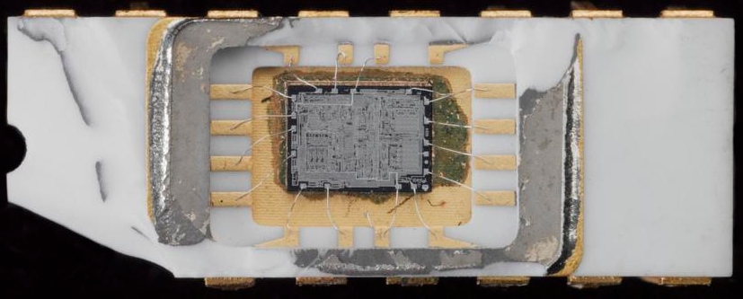
. Intel 4004 Delidded (Image Courtesy Science Museum Group Collection Online – CC BY-SA 4.0)
Because the 70s, there have actually been a number of advancements in substrate developed. Metal frames paved the way to traditional ceramic chip in the 90s, and after that natural product packaging around the turn of the centuries. Each model of substrate had much better homes than the last, above all else, making it much easier to path a bigger variety of signal and power pins to progressively intricate passes away.
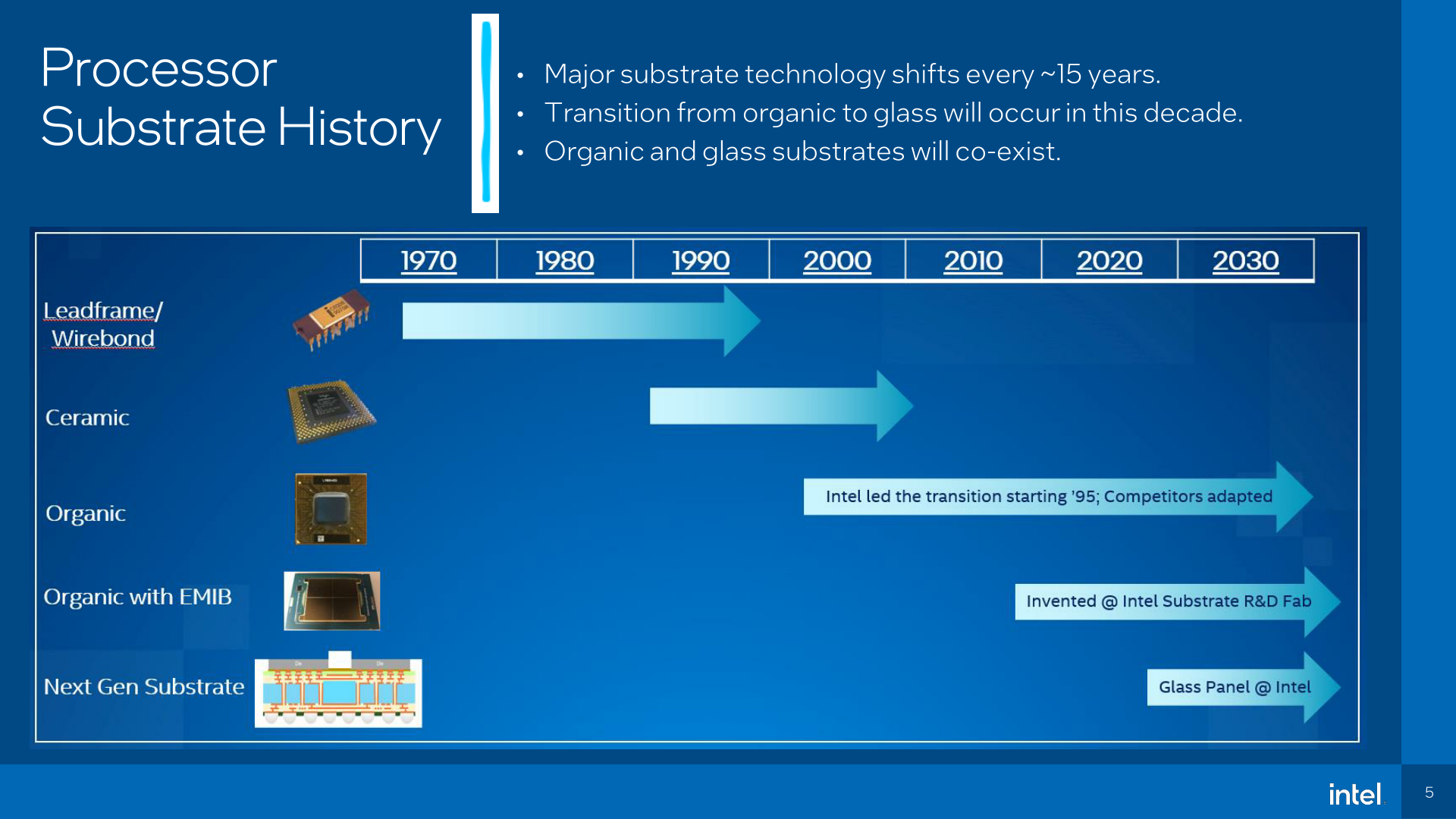
While you’ll still discover lead frame and ceramic chips occasionally, natural substrates have actually been the support of the market for the last number of years. The natural product, basically made from PCB-like product layered with woven glass laminates, permits a relatively a great deal of signals to be routed through a chip, consisting of standard chiplet styles such as Intel’s mobile processors (with PCH different PCH and CPU passes away) along with AMD’s chiplet-based Zen processors.
However natural substrates have actually currently been a restricting element for a long time now, particularly in high-end chips. Which is why over the last years we have actually seen the increase of ultra-high-density adjoin user interfaces such as silicon interposers (chip on wafer on substrate), and their derivatives like Intel’s own EMIB. These have actually enabled business to bridge together the important courses of their chips with quick and thick pieces of silicon, however at relatively high expenses, and without completely dealing with the downsides of natural substrates. As an outcome, Intel has actually likewise been looking for a real replacement for natural substrates, one that will play well with big chips, and while not changing the requirement for CoWoS/EMIB at the greatest level, would provide much better signal efficiency and denser routing than natural substrates today.
Glass Core Substrates: Finer, Yet More Powerful
This brings us to the subject these days’s statement from Intel, glass core substrates. The business has actually been dealing with changing natural substrates with glass for over a years now, and they have actually lastly reached the point of development where they’re all set to reveal it off to the world while preparing for its usage in future items.
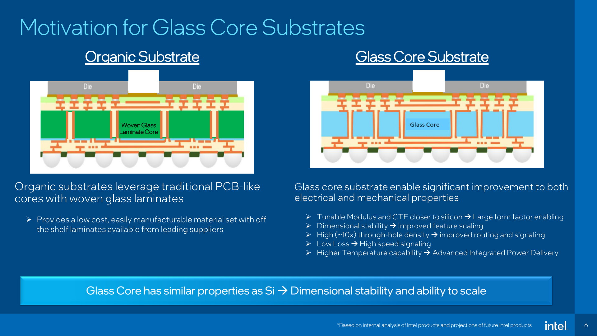
At a high level, a glass core substrate is simply that: changing the natural, PCB-like product of a natural bundle with glass. To be sure, this does not indicate changing the whole substrate with glass– so Intel is not going to be installing chips on pure pieces of glass– however rather, the product at the core of the substrate would be made from glass. On the other hand, metal redistribution layers (RDLs) would still exist on both sides of a chip, offering the real paths in between numerous pads and solder joints.
. Glass Core Substrates In Panel Kind
While more difficult to deal with than the now reputable natural substrate, Intel thinks about glass substrates to be exceptional both in mechanical and electrical homes, which in turn makes them preferable to utilize in future chips. Or, on the other hand, less unfavorable than natural substrates when constructing huge chips.
Beginning with the mechanical side of matter, Intel reports that glass core substrates provide far much better mechanical strength than natural substrates. They have the ability to stand up to greater temperature levels much better than natural substrates throughout product packaging, leading to less warping and distortion. Glass is likewise supposedly much easier to get flatter too, that makes product packaging and lithography much easier. Lastly, glass has a comparable coefficient of thermal growth as silicon (unlike natural substrates), suggesting that what little bit deforming that still takes place from heat follows the passes away above, instead of having various parts of a chip broadening at various rates.
Most notably, possibly, is that all of those products taken together open the door to producing bigger chips. With a more steady substrate to install the passes away on, it will be possible to have bigger passes away and a bigger variety of passes away all sharing a single substrate– and therefore acting as a single chip.
Bridging the space in between mechanical and electrical, according to Intel, they’re likewise able to attain a much tighter pitch on the through-glass vias (TGVs) that bring signals through the substrate itself, enabling a much bigger variety of vias in general. Intel is reporting that they have the ability to area TGVs less than 100 microns ( µm )apart, enabling a 10-fold enhancement in TGV density. All of which eventually permits more versatility in routing signals through the substrate core, and to some degree makes it much easier to path signals with less RDL layers.
.
Put Together Test Chip Substrates
All of this, in turn, permits not just bigger chips, however for more passes away to be put on a same-sized chip. According to Intel, glass product packaging would enable them to put 50% more passes away on a chip– or rather, the die complex location within a chip might be 50% bigger– enabling more largely jam-packed chips than what Intel can do today.
Lastly, on the electrical side of matters, glass core substrates, and more particularly the TGVs, supposedly provide much better electrical efficiency too. Owing to the low loss nature of the dielectric utilized in TGVs integrated with the much bigger variety of them, Intel states that glass core substrates will permit cleaner signal routing and power shipment. When it comes to the previous, that implies having the ability to do 448G signaling through copper, instead of needing to utilize optical interconnects. On the other hand, lower-loss power shipment would enhance total chip effectiveness by that a lot more, by decreasing the quantity of energy that is lost as heat prior to it even reaches the processor passes away.
Further down the line still, glass core substrates ought to likewise make co-packaged optics much easier to achieve for when you do wish to utilize optical. A glass substrate would permit optical interconnects to be incorporated right into the chip, instead of needing to tack it on in other good manners.
So if glass is so fantastic, what’s the catch? While Intel is naturally more fired up to speak about what’s excellent about glass core substrates and what they have actually discovered works well so far, one inevitable component will be expense. Like any brand-new innovation, glass core substrates will be more costly to produce and package with than attempted and real (and low-cost) natural substrates. And while Intel isn’t speaking about yields this far out, it will be tough for glass to take on natural, a minimum of in the beginning.
More broadly speaking, glass core substrates likewise implies that Intel requires to bootstrap a total community for the product. They aren’t vertically incorporated with natural substrates today, and they will not be vertically incorporated with glass, either. To that end, Intel is currently dealing with partners today to establish the required tooling and supply capability, to bring themselves to preliminary industrial production. However over the longer-term, Intel will require to determine how to make outsourced screening and assembly possible, particularly as Intel prepares to provide glass core substrates to IFS consumers in the future.
Lastly, it bears keeping in mind that while glass core substrates permit a tighter signal pitch than natural substrates, they are not a replacement for EMIB, Foveros, or other advanced packaging methods based around utilizing silicon mediums. A 75µm pitch for a TGV is still a far cry from the 45µm pitch of EMIB, never ever mind the << 10µm pitch prepared for Foveros Direct. So all of those product packaging innovations will stay complementary add-ons to glass core substrates, at finest changing EMIB in fringe cases of items that do not require the complete density enhancements of EMIB.
Glass In Action: Intel’s Completely Practical Test Chip
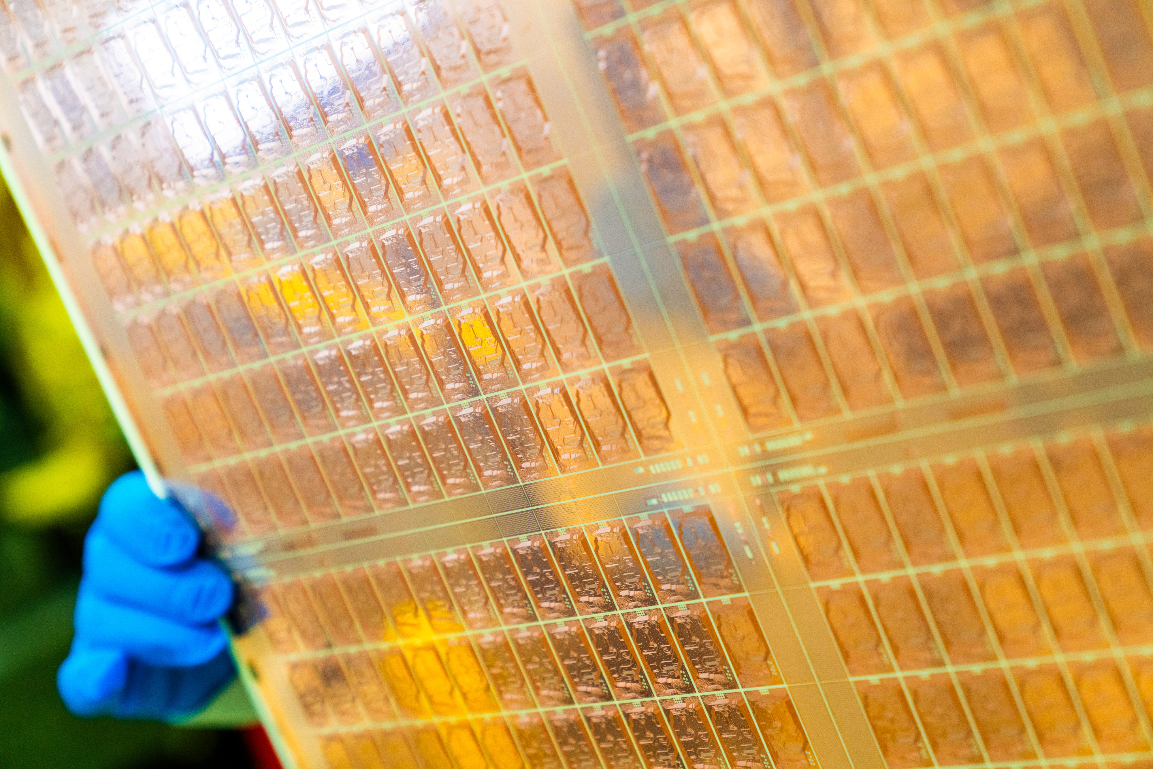
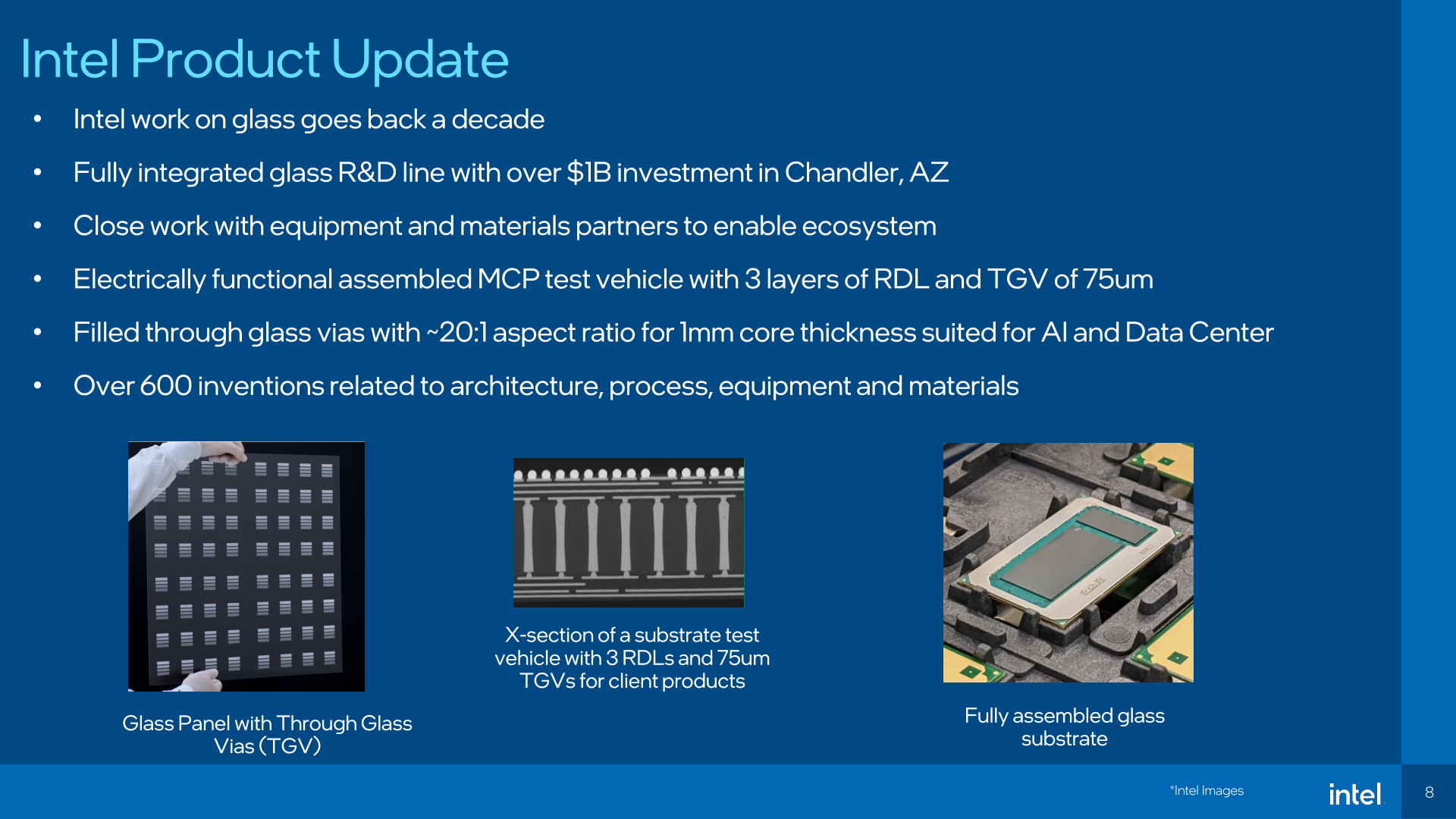
The last part of today’s statement from Intel is based around the production side of matters. As kept in mind previously, Intel has actually been dealing with glass core substrates for over ten years now, and more just recently has actually been starting a three-and-a-half-year pathfinding task to bring glass core substrates to the next action. Support those efforts, at this moment the business has actually a completely incorporated R&D line up and running in among their Chandler, Arizona fabs (the very same one that does EMIB). Entirely, Intel has actually invested over a billion dollars on glass core R&D so far.
The very first fruit of their R&D efforts, Intel has actually finished the assembly of a set of test automobiles– multi-chip plans constructed over a glass substrate. The chips, which look comparable to Intel’s ultra-low power mobile chips (Alder Lake-U 9W?), are supposedly totally practical, offering Intel some useful outcomes to report on. While we do not have a lots of information on the chip, Intel has actually informed us that it utilizes 3 layers of RDL, and the TGVs have a pitch of 75µm.
Together with showing the electrical homes of glass, the little test chip is likewise meant to show a few of the physical homes, too. The glass core was made really thick– on the order of 1mm– in order to show that TGVs would deal with such a thick core. For the type of enormous, high-end chips Intel is intending on utilizing glass core packaging for, those chips will need an extremely thick core in order to strike their size objectives, so Intel required to show that TGVs would (still) work at such lengths.
Intel Glass Core Substrates: Coming Later On This Years
Covering things up, today’s statement acts as a kick-off of sorts for Intel’s glass core substrate period. Following on their years of R&D work and their pathfinding sprint, Intel now thinks they are all set to start preparing for the shift to glass core substrates in their items– albeit a shift that is still a number of years out.
If Intel’s item advancement goes according to strategy, the business plans to start delivering glass core items later on this years. The very first items to get the glass core substrate treatment would be their biggest and most lucrative items, such as high-end HPC and AI chips. These are the items most strained by the usage of natural substrates today due to the size restricts those substrates enforce, and those are the limitations intel thinks would most gain from glass core product packaging.
Longer-term, the strategy is to waterfall down the innovation from HPC chips into smaller sized and smaller sized chips, up until the innovation is offered (and feasible) for Intel’s rank and file customer chips. The business is really fast to keep in mind that glass and natural substrates will co-exist for many years to come– and, like previous shifts, there will likely still be chips utilizing natural substrates well after glass is presented– however the business is likewise positive that they’ll have the ability to bring the expenses of glass core substrates to parity with natural substrates, ultimately making it possible to profit even in lower-priced processors.
And Intel will not be keeping the innovation to themselves, either. As part of the business’s wider effort to end up being a world class agreement foundry, Intel will be using glass core substrates to IFS consumers in due time. While it’s far prematurely to think when that would be (even Intel items might be 6 years out), having the ability to provide glass product packaging might offer Intel a huge upper hand over its rivals, particularly for producing high-end, highly-profitable chips.
Above all else, it requires to be repeated that there’s a good deal of work Intel still requires to do in order to bring glass core substrates to the marketplace. However if the business succeeds, then the switch to glass will introduce the type of significant innovation shift that just occurs every 15 to twenty years.